


 (1)-Photoroom.png "For engineering and management programs")


Latest events & happenings
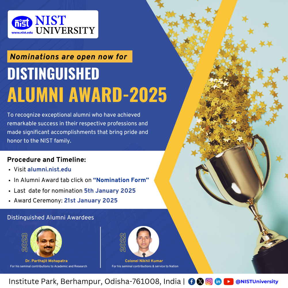
Experience holistic learning with a student first approach
15
SEPT
NIST University proudly observed the 58th Engineers’ Day with immense enthusiasm and reverence at the Stephen Hawkins Cineplex, paying tribute to the legendary Bharat Ratna Sir M. Visvesvaraya, whose vision and contributions continue to inspire generations of engineers. The celebration was graced by Ch. Netaji Subudhi, Chief Engineer, hashtag#TPSODL, who joined as the Chief Guest. In his keynote address, he delivered an impactful lecture on the hashtag#PMSuryaGharYojana, shedding light on its benefits, scope of application, and practical guidelines. His insights not only highlighted the role of engineers in advancing hashtag#renewableenergy but also encouraged hashtag#NISTians to actively participate in building a sustainable future. Our Hon’ble Vice Chancellor, Prof. Priyadarsan Patra, spoke on the significance of Engineers’ Day, reflecting on Sir M. Visvesvaraya’s pioneering work and his timeless contribution to Indian engineering and nation-building. Adding depth to the occasion, Dr. P. Rajesh Kumar (rajesh panakala), Dean of Academics emphasized the importance of celebrating this event in a technical university, reminding budding engineers of their responsibility in shaping modern society through innovation and ethical practice.
13
SEPT
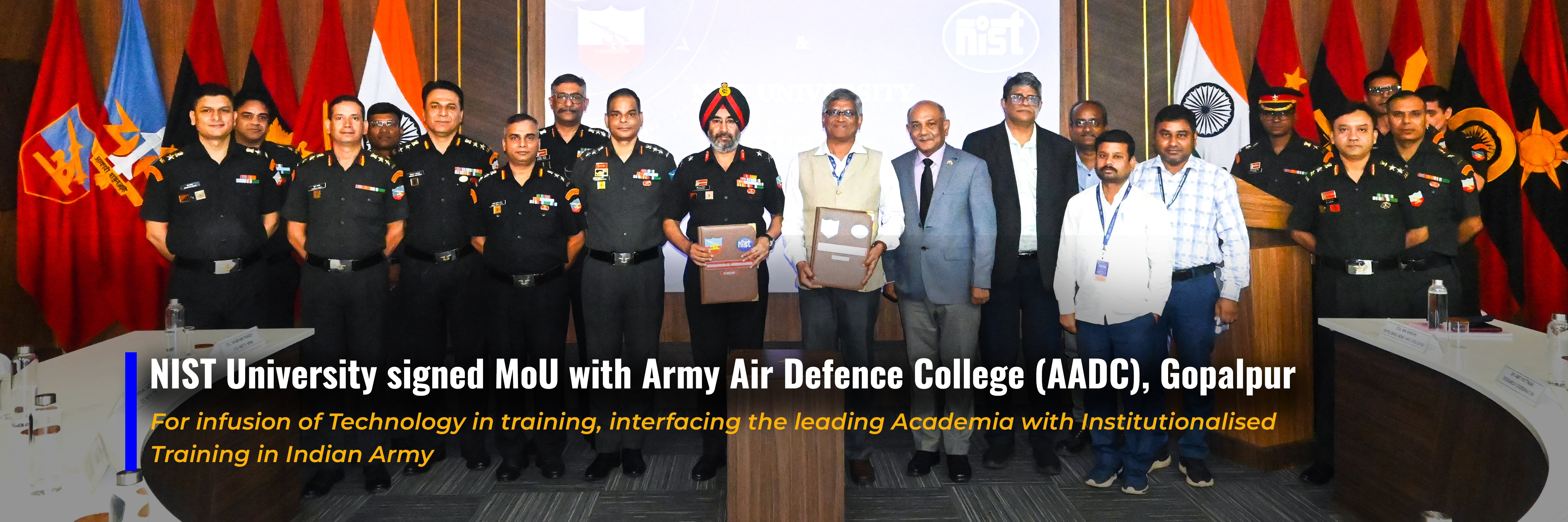
NIST University proudly signed a Memorandum of Understanding (MoU) with the Army Air Defence College (AADC), Gopalpur, under the aegis of hashtag#ARTRAC, marking a significant step in strengthening Academia-Defence collaboration. This partnership is aimed at infusing cutting-edge technologies into hashtag#defencetraining, with a focus on Artificial Intelligence & Machine Learning (AI & ML), hashtag#5GTechnology, and Advanced Electronics. The collaboration will further pave the way for joint research and development, faculty-student exchanges, guest lectures, and technical seminars, creating a vibrant platform for innovation and knowledge sharing. A proud milestone for NIST University, this initiative brings hashtag#academia and hashtag#defence together to drive forward research, skill development, and national service through technology-led contributions.
10
SEPT
A Mega Tree Plantation Program was organized at the NIST University campus by the Odisha Environment Society with the support of the State Bank of India. The program was formally inaugurated by Dr. Sukant K. Mohapatra, Our Hon’ble President. The distinguished guests of the occasion included Mrs. Vaishali Sharma, Branch Manager, SBI, Golonthara Branch, and Dr Bishnukar Nayak, Registrar (I/C), NIST University. The initiative aims to plant 1,500 saplings of diverse species such as Ashoka, Arjun, Neem, Karanja, Amla, Krushna Chuda, Kadamba, Custard Apple, Jamun, Pomegranate, Muchukund, Bael, Sirisha, and more across the campus
09
SEPT
NIST University was honored to host Mr. Venkata Narasimham Peri, CEO of CognitiveCare, USA, on our campus. Cognitive Care is a pioneering company working in preventive hashtag#healthcare, drug discovery, analytics, and cutting-edge projects in pharma and life sciences. During his visit, Mr. Peri engaged in an insightful interaction with our faculty members and students, sharing his expertise and perspectives on the future of healthcare innovation. He explored the Artificial Intelligence Global Innovation Center (GIC), where he witnessed the demonstration of our AI-based Pediatric Pneumonia Detector. Mr. Peri also highlighted several innovative challenges in AI-driven healthcare and encouraged our students and faculty members to explore impactful solutions in this domain.
08
SEPT
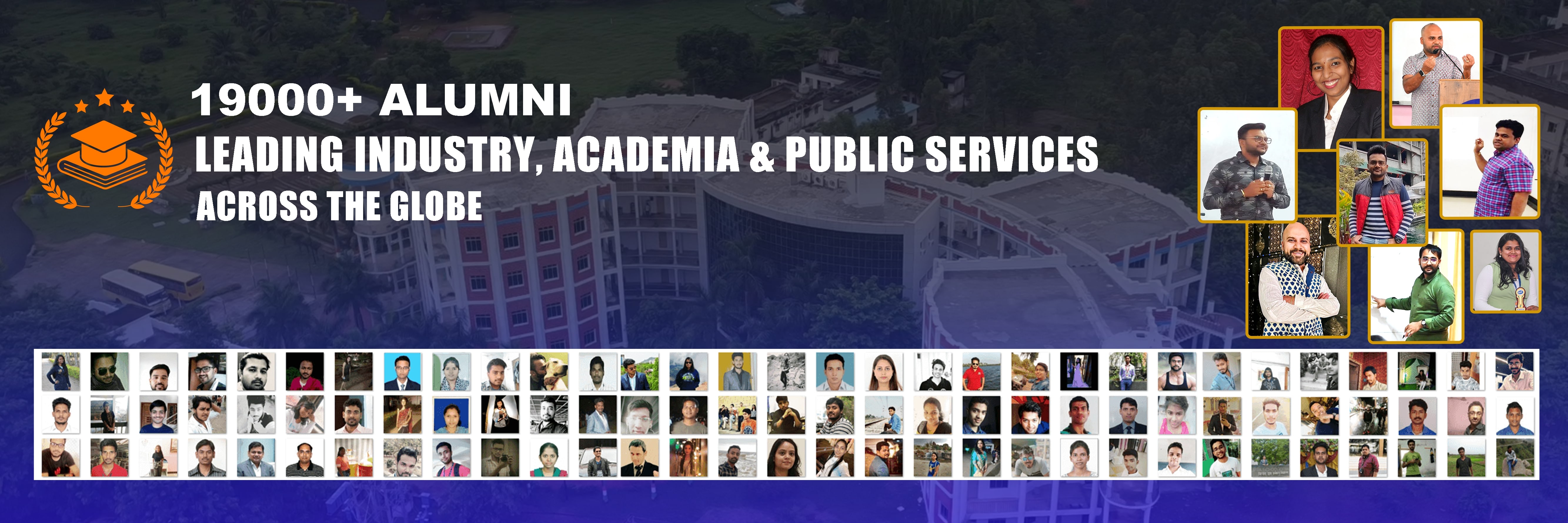
NIST University recently organized a Faculty Induction Program to welcome and orient its newly joined faculty and staff members. The program aimed to familiarize the new members with the university’s legacy, vision, academic culture, and professional ethos, ensuring they feel seamlessly integrated into the NIST community. The program was graced by our Hon’ble President, Dr. Sukant K. Mohapatra, who shared the inspiring journey of hashtag#NIST, its history, and the university’s mission and vision for the coming decade. He highlighted the academic and research facilities, campus infrastructure, student achievements, and the strength of our 19,000+ global alumni network, underscoring the proud legacy that NIST carries forward. Prof. Priyadarsan Patra, Vice Chancellor, introduced the university’s leadership structure.
06
SEPT
NIST University proudly congratulates Dr. Abinash Dutta, Assistant Professor, Department of Biotechnology, on being honored with the prestigious Dr. A.P.J. Abdul Kalam Memorial Award 2025, presented by the Research Council of India (RCI). This distinguished recognition celebrates Dr. Dutta’s exceptional contributions to hashtag#academics and hashtag#research, reflecting his unwavering commitment to hashtag#knowledgecreation, hashtag#innovation, and hashtag#academicleadership. His work embodies the vision and values of Dr. A.P.J. Abdul Kalam - the People’s President and an enduring symbol of modern India’s scientific and educational advancement. Dr. Dutta’s achievement is not only a personal milestone but also a proud moment for the entire NIST community, inspiring students, faculty, and researchers alike to pursue excellence and innovation.
05
SEPT
NIST University proudly celebrated Teachers’ Day at the Stephen Hawking Cineplex, honoring the invaluable contributions of its faculty and staff. The event was marked with heartfelt tributes, inspiring speeches, and moments of joy that reflected the true spirit of teaching and learning. Dr. Sukant K. Mohapatra, our Hon'ble President, highlighted the significance of Teachers’ Day and shared some of the remarkable milestones achieved by the faculty in academics and research. He emphasized how teachers are the true pillars of nation-building, nurturing not just knowledge but also values. Prof. Priyadarsan Patra, our beloved Vice Chancellor, fondly remembered great teachers who shaped the history of education, including Dr. Sarvepalli Radhakrishnan, Chanakya, and others. He stressed that every teacher carries forward their legacy by guiding and inspiring the next generation.
03
SEPT
NIST University stands united for a brighter, healthier future. As part of the Nasha Mukt Bharat Abhiyaan, we pledge to create awareness, inspire positive choices, and build a society free from the grip of substance abuse. Join us on 13th August 2025 to take the Mass Pledge Against Drug Abuse at https://nmba.dosje.gov.in and be a voice for change. Together, let’s choose life, health, and hope over drugs.
21
AUG


